


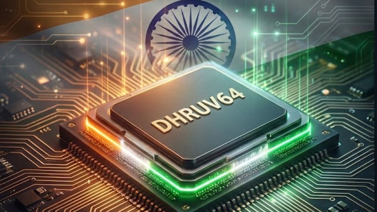
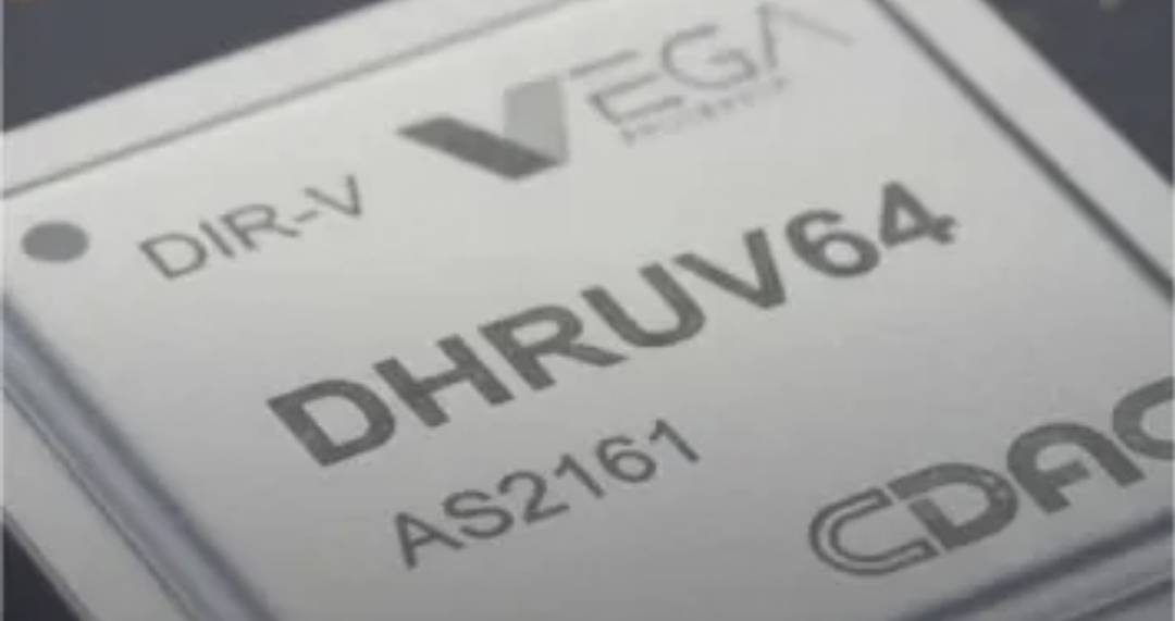
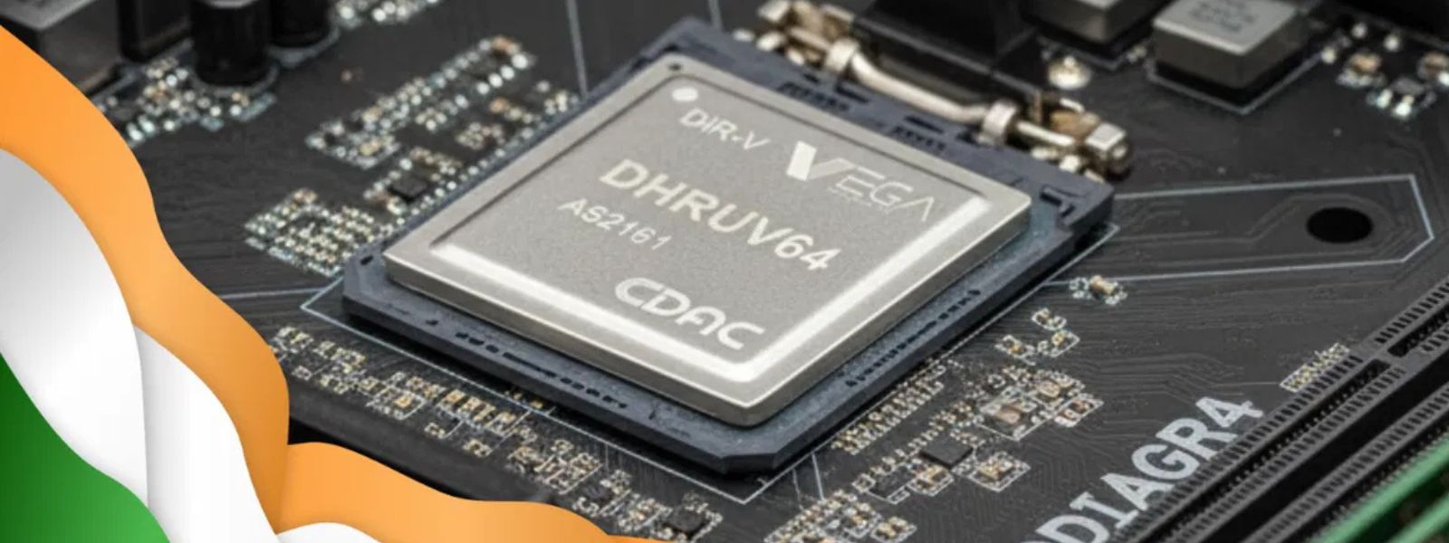
India Launches DHRUV64, First Indigenous 64-Bit Dual-Core Processor

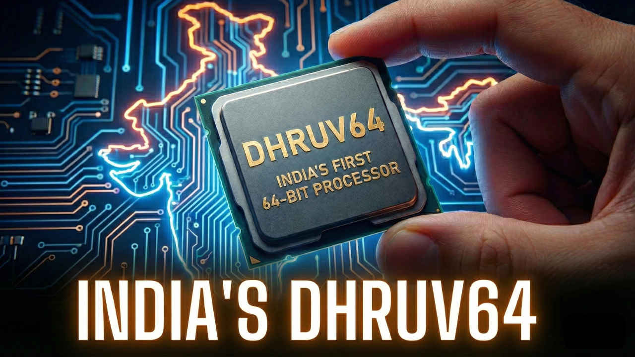
India has reached a major milestone in semiconductor self-reliance with the development of DHRUV64, the country’s first indigenous 1.0 GHz, 64-bit dual-core microprocessor. Developed by the Centre for Development of Advanced Computing (C-DAC) under the Microprocessor Development Programme, the processor marks a critical step in reducing dependence on foreign chipmakers for strategic and commercial technologies.
Design and Architectural CapabilitiesDHRUV64 is built on a modern 64-bit dual-core architecture designed to deliver higher computational efficiency, enhanced multitasking and improved system reliability. Operating at a clock speed of 1.0 GHz, the processor is suitable for demanding workloads while maintaining energy efficiency. The design enables seamless integration with a wide range of external hardware systems, making it adaptable across multiple technology domains.
What Comes After DHRUV64
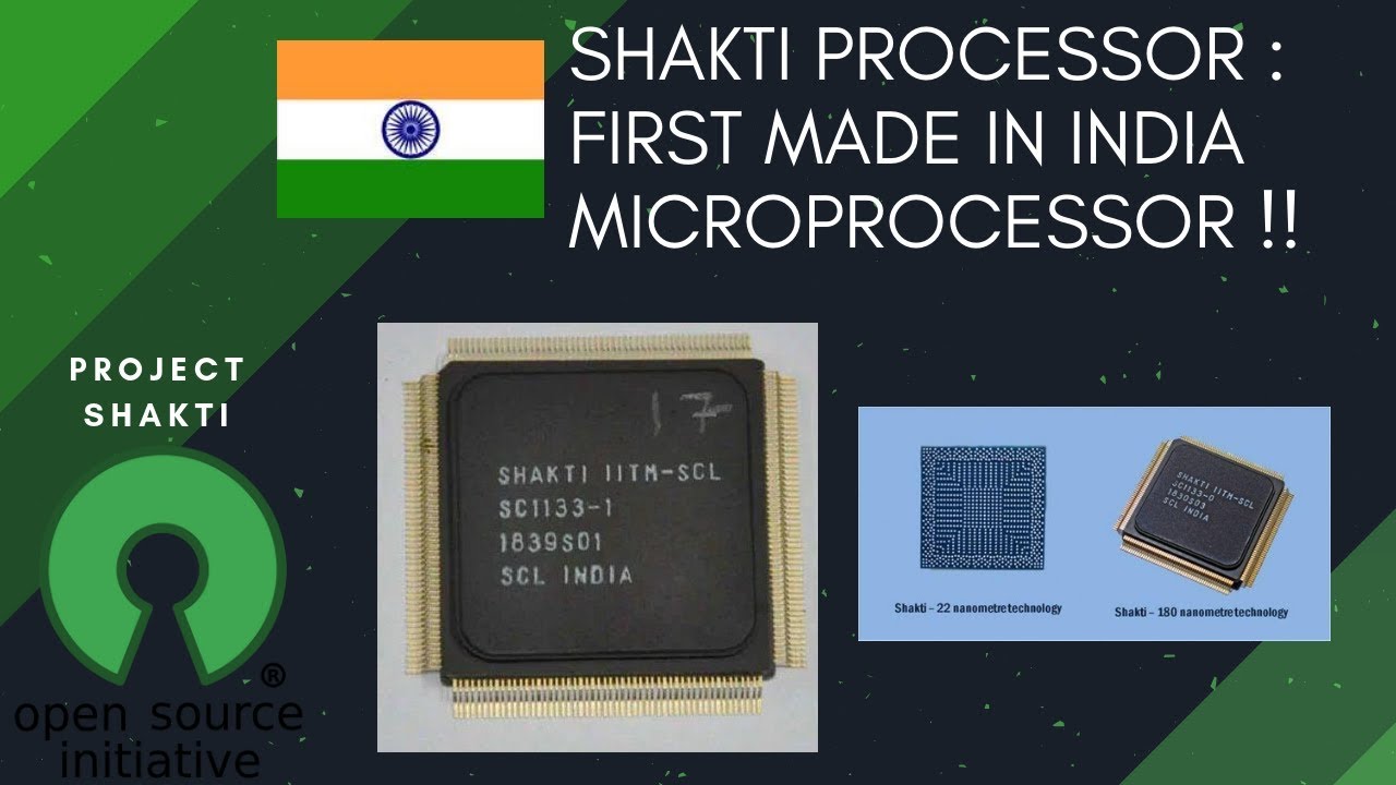
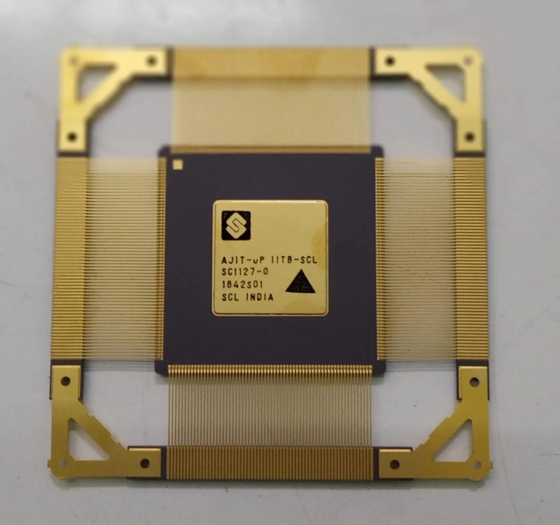
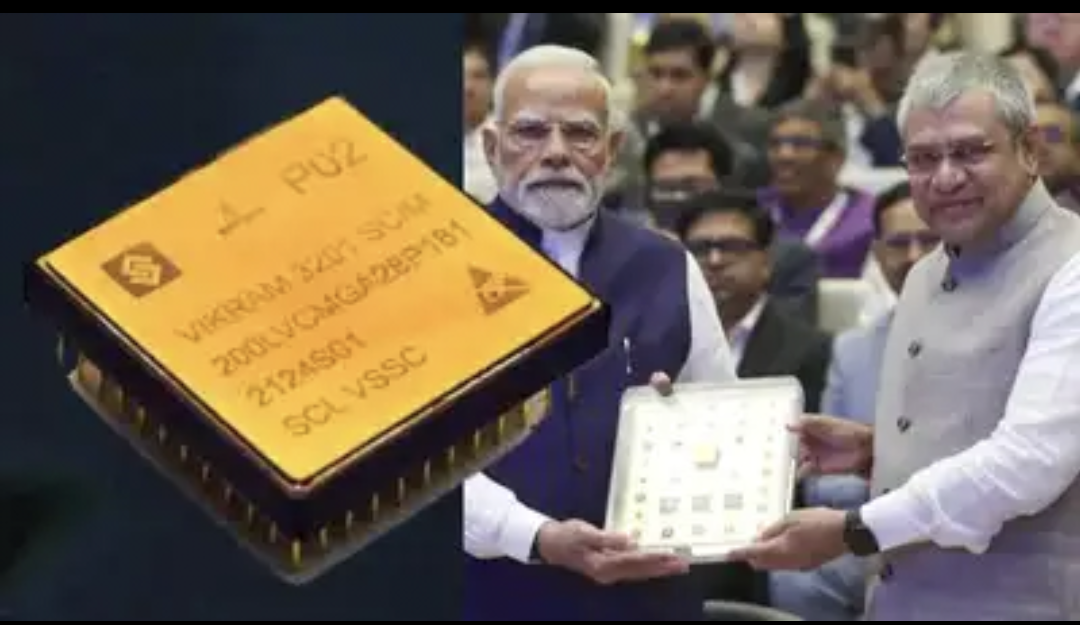
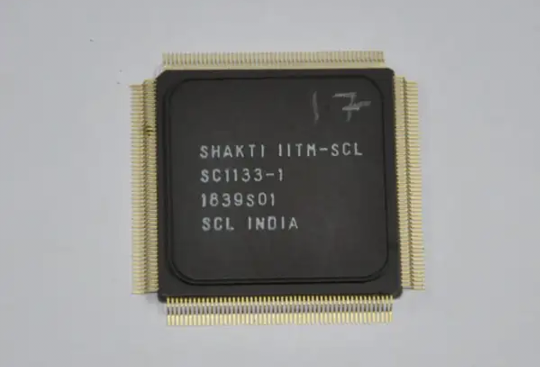
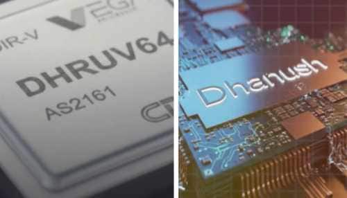
DHRUV64 joins a growing family of India-developed processors, including SHAKTI from IIT Madras, AJIT from IIT Bombay, VIKRAM engineered for space applications, and THEJAS64 for industrial automation. Building on this momentum, C-DAC is working on next-generation RISC-V based system-on-chips, Dhanush and Dhanush+, aimed at expanding indigenous options for both strategic and commercial use across sectors.Feeling proud in expanding our capabilities.I hope in future it will plug the gap that still exists in the processing equipments, sensors and environment management for manufacturing these processors.I often found many equipments imported as not available in india, but are much easier to make than a processor development.
Decoding the architecture
At the CPU level, DHRUV64 implements a 64-bit RISC-V instruction set with dual VEGA AS2161 cores. The design supports single- and double-precision floating point, a hardware MMU and Linux execution. The microarchitecture uses a 16-stage out-of-order pipeline, includes advanced branch prediction, and supports user, supervisor, and machine modes, placing it in the application-class processor category rather than the microcontroller class.Libin said the design goal was to progress in a controlled and manageable way. Jumping directly from earlier 32-bit processors operating in the tens of megahertz range to a multi-gigahertz, multi-core design would have introduced too many variables at once. “That would have been an exponential jump,” he said. “So, we treated DHRUV64 as an intermediate milestone.”
The memory subsystem is sized for embedded Linux workloads, with 128 KB of SRAM, a DDR4 memory interface and a quoted 75.4 GB/s memory interconnect bandwidth. This points to an emphasis on internal data movement rather than clock frequency alone. A low-latency vectored interrupt controller supports mixed real-time and Linux environments.Some intellectual property blocks, such as DDR memory interfaces, were licensed and integrated as minimum essential components, while the overall system architecture remained indigenous,” Libin said. “The intent was to deliver a complete and demonstrable platform rather than an isolated CPU core.”
From a system integration perspective, DHRUV64 includes a wide range of peripherals, such as PCIe, SATA, USB 2.0 host and device, Ethernet MACs, SD/eMMC, DMA, a display controller, a camera interface, GPIOs, UARTs, I²C, SPI, PWM and timers. The interface breadth positions the chip as a central embedded computing platform rather than a companion processor.The design also allows external expansion through a static memory controller interface. “If a required protocol is not supported natively, system designers can attach an external FPGA and communicate through that interface,” Libin said.
Software support includes Linux compatibility, standard storage and networking controllers, and a full memory subsystem. The processor operates at 1 GHz with 1.8 V I/O, placing it in the industrial and infrastructure segment rather than power-constrained mobile devices.Real-time behavior is currently being verified through a combination of pre-silicon and post-silicon testing. Before fabrication, peripherals like SPI, I²C and UART were exercised in laboratory environments. Differences between test platforms and silicon are expected.“On the actual chip, Linux can boot in about two seconds,” Libin said. “In the test environment, it may take one or two minutes.”Verification has also relied on FPGA-based prototyping and emulation platforms to debug issues at different stages of development, he added.
Moving beyond the test stage
Libin cautioned against treating the 1 GHz figure as a final performance claim. DHRUV64 is currently a test chip undergoing extensive validation. “This is the first chip, and we are testing it in our lab,” he said. “A refined version may go to the market later.”Much of the current validation work involves operating the processor at significantly lower frequencies. “In test setups, we run it at around one-twenty-fifth of the target frequency,” Libin said. “At that level, we can verify basic functionality. When you go to the actual frequency, you need to validate timing, interfaces, and application-level behavior.”The chip is targeted at applications including industrial automation, IoT and smart devices, networking equipment, consumer electronics, automotive systems, medical electronics, Wi-Fi routers, single-board computers, and biometric access control. Mobile, GPU-heavy or AI-accelerator-centric use cases are not emphasized.
Libin said comparisons with other application-class processors should be made cautiously. Architectural differences, such as execution models and internal pipelines, often make direct performance comparisons misleading. “It is not an apple-to-apple comparison,” he said.C-DAC said the processor is intended for use by academia, startups, and industry working on embedded and edge computing systems. Early adopters are expected to require detailed documentation and reference designs, though engineers familiar with Arm-based platforms are likely to find the transition manageable.

“Indigenous will not always sell,” Libin said. “Engineers will choose a chip based on technical reasons.” He pointed to the number of supported interfaces in DHRUV64 as a practical advantage for embedded Linux systems that require limited connectivity.Access to the platform remains limited as the validation stage continues. Evaluation units are not yet available to companies, though broader access may follow once testing is completed.C-DAC is also working on next-generation SoC designs named Dhanush and Dhanush+.DHRUV64 follows earlier Indian processor efforts led by academic and government institutions. These include SHAKTI from IIT Madras and AJIT from IIT Bombay, both introduced in 2018. More recent processors include VIKRAM, developed by ISRO and Semiconductor Laboratory for space applications, and THEJAS64 from C-DAC for industrial use..
INFORMATION CREDIT : Google
Follow For More : @TESVIPER10
I QUEST ON AND ON 🖤 💛
Please sign in
Login and share